|
ФњЕБЧАЕФЮЛжУЃКЪзвГ >> ВњЦЗеЙЪО >> ЙтЦзвЧЯЕСа - Л№ЛЈжБЖСЙтЦзвЧ |
|
| |
Multi-layered graphene sample | |
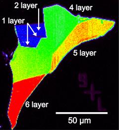 |
Graphene monolayer, bilayer and other multiple-layer regions identified
StreamLine™ Plus image showing the distribution of different thicknesses within a graphene flake
Map area: 110 µm x 120 µm
Spectra generated: 40,000
Acquisition time: 14 minutes |
CVD diamond film |
|
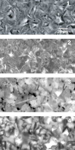 |
Polished surface of polycrystalline diamond film grown by CVD technique
Images show information on crystal shape, orientation, stresses and defect densities
Map area: 175 µm x 88 µm
Spectra generated: 51,200
Acquisition time: 2 imaging experiments, 15 minutes each (first acquisition used to generate three Raman images, second acquisition used to generate photoluminescence image)
Image 1: Raman image showing 1 cm-1 variation in position of the 1332 cm-1 diamond band
Image 2: Raman image showing 2 cm-1 variation in width of the 1332 cm-1 diamond band
Image 3: Raman image showing variation in peak area of the 1332 cm-1 diamond band
Image 4: Photoluminescence image showing variation in the intensity of the 1.68 eV neutral silicon vacancy [Si-V]0 band |
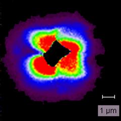
Micro indentation in silicon wafer |
|
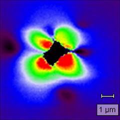 |
Peak position
Peak position derived from curve-fit analysis
Map area: 10 µm x 10 µm
Spectra generated: 10,000
Acquisition time: 36 minutes (single acquisition analysed for both images)
Scan details: 100 nm step achieved using piezoelectic scanning stage |
 |
Peak width
Peak width derived from curve-fit analysis |
Sandstone from Loch Torridon, Scotland |
|
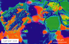 |
StreamLine™ Plus image showing the distribution of Anatase (TiO2) (red), Quartz (SiO2) (green) and Haematite (Fe2O3) (blue)
Area of section: 500 µm x 320 µm
Spectra generated: 67,200
Acquisition time: 20 minutes |
Polymer laminate (PS and PMMA) |
|
 |
StreamLine™ Plus image of polymer laminate sample showing the distribution of PMMA (red), Epoxy (green) and PS (blue)
Map area: 240 µm x 645 µm
Spectra generated: 17,200
Acquisition time: 7 minutes |
Strained S-Ge cross-hatch |
|
 |
StreamLine™ Plus image of a Si-Ge semiconductor sample exhibiting a strained structure. The map shows variation in the Si-Si 510 cm-1 band position (~0.2 cm-1 positional band shift). The map data was generated using curve fitting.
Map area: 129µm x 130µm
Spectra generated: 55,000
Acquisition time: 13 minutes |
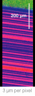
Tooth section |
|
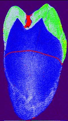 |
StreamLine™ Plus image of a sectioned tooth, highlighting the enamel (green), dentine (blue) and areas of high fluorescence (red)
Map area: 9mm x 16mm
Spectra generated: 84,000
Acquisition time: 20 minutes |
| Multilayred graphene sample | |
| |
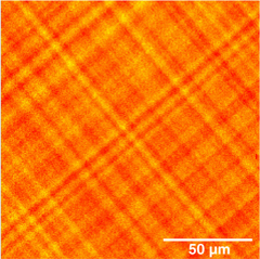
Laser induced crystalline silicon tracks | |
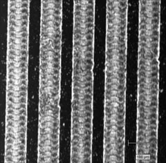 |
StreamLine™ Plus image of laser induced crystalline silicon tracks on amorphous substrate
Map area: 550µm x 550µm
Spectra generated: 70,000
Acquisition time: 17 minutes |
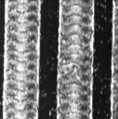 | Zoomed region (~ 250µm x 250µm) of above image |